Technology
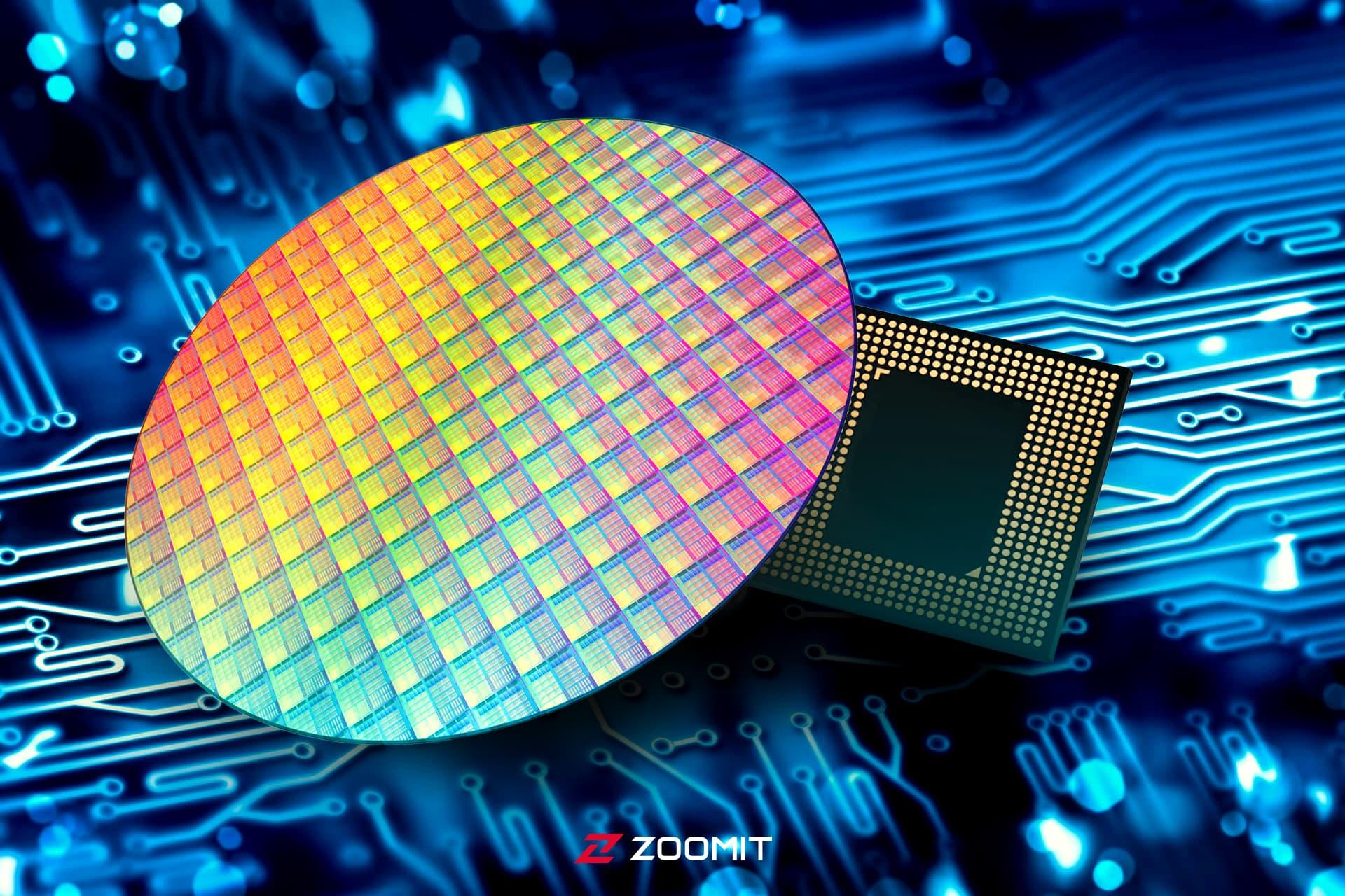
Designed in California, copied in the Soviet Union; The story of the first Soviet chip
Designed in California, copied in the Soviet Union; The story of the first Soviet chip
During the Cold War, the United States and the Soviet Union were engaged in a breathtaking competition in various fields, and each tried to prove its ideological superiority by showing its progress. This competition was not limited to the battlefield and extended to space, nuclear capabilities, technological innovation, and even competition to discover new super-heavy elements.
The space race, which culminated with the launch of the Sputnik satellite by the Soviet Union and the United States’ Apollo landings on the moon, attracted everyone’s attention and became a symbol of the Cold War at that time. Similarly, the arms race led both superpowers to amass and develop advanced nuclear arsenals, a constant reminder of the unstable balance of power. This extensive competition fueled technological advancements in the military and space fields and influenced the process of innovations.
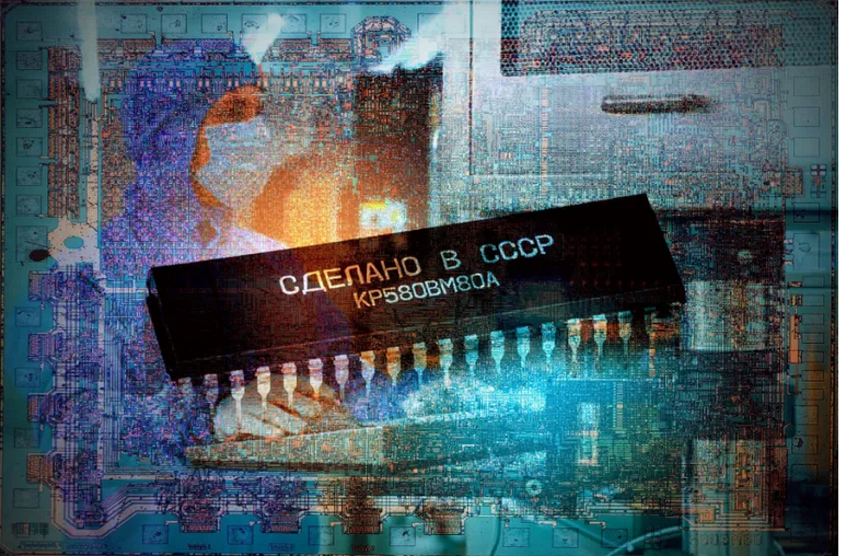
One of the examples of this technology competition was the development of computer technologies. In the early 1970s, the Soviet Union began to imitate key Western innovations in the field of microprocessors, aiming to close its technological gap with the West. One of these innovations was the Intel 8080 microprocessor, which was considered a significant development in the computer field. The Soviet version of the 8080, known as the KR580VM80A (aka the 580 series), represented their broader strategy of reproducing Western technology.
This competition for copying and innovation during the Cold War illustrates the interplay between geopolitical conflicts and technological advances. Due to the silence of news in the Soviet Union at that time, little has been written about the details and the story behind this processor. In this article, by examining most of these sources, we are trying to discuss the story of the design and introduction of the Russian copy of the 8080 microprocessor.
Soviet Union before the Silicon Age
Before going into the history of the Soviet 580 series microprocessors, it is necessary to briefly talk about the level of Soviet technology before the emergence of integrated microprocessors.

In 1950, the “Small Electronic Computing Machine” (SECM) was developed in the Soviet Union. It should be noted that SECM was launched in the Soviet Union when there were only a few computers in Europe; including the English EDSAC, which had been launched a year earlier, and the Z4 Zuse in Zurich, which had been built around 1947. However, the SECM processor was much more powerful because it processed the calculations in parallel.
In the construction of SECM, all the basic principles of computer construction, such as the presence of input and output devices, coding and storing the program in memory, automatic execution of calculations based on the stored program, and other such things, were used. Most importantly, this computer was built on binary logic (processing based on zeros and ones) used in digital computing engineering.
 Large Soviet BESM-6 electronic calculating machine at the London Science Museum
During the historic Soyuz-Apollo space mission in 1975, mission control was handled by a complex system that included a large computer called the BECM-6 (Big Electronic Computing Machine). This computer was developed directly from SECM and was able to perform the calculations needed to launch a missile in one minute; While on the American side, the calculations related to this mission lasted 30 minutes. This time difference in calculations indicated the technological differences between the two countries at that time.
So far, Soviet computing superiority over the West has been evident. But the real disaster occurred when the Soviets decided to produce copies of the IBM-360 mainframe computer; It meant the transition from innovation to copying American design. It is clear that copying does not stand a chance of being overtaken; However, the Soviets usually upgraded Western designs to make them look more indigenous and innovative.
The Soviet SECM performed calculations in one minute, but the American computer in 30 minutes
Copying only makes sense when it is used as a learning step in the absence of technology necessary for innovation. Of course, the logical end of such an approach is still moving towards the development of dedicated systems, which today, China has clearly demonstrated the effectiveness of this method. However, this story did not have a happy ending for the Soviet Union. From the moment the decision to copy was made, the Soviet Union was in an impossible scramble for advancement in the chip industry.
Copy instead of innovation
In late 1962, by order of the Soviet Union government, the Kyiv Design Bureau was established in the capital of the Ukrainian Socialist Republic, later known as the Kyiv Institute of Micro Devices (KNIIMP). This institution was associated with an experienced manufacturing plant. In August 1976, the institute’s first official mission was to create a copy of the Intel 8080 microprocessor, which had only been introduced for two years.
The design team of the KR580VM80A processor included a group of talented engineers and specialists working under the supervision of the Electronics and Engineering Design and Research Center. The team, led by Nikolai Beretsky, one of the most prominent Soviet engineers at the time, was responsible for the design and development of the new processor.
At the beginning of the work, the design team faced problems such as a lack of resources and advanced equipment. In particular, the production of semiconductor products in the Soviet Union faced serious problems due to the limitations of technology and raw materials, which directly affected the quality and performance of the processor. These issues caused delays in the project and the need for adjustments in the design.
 Kiev Institute of Micro Devices with strange architecture during the Soviet era
On the one hand, funding technology projects during the Cold War was a big challenge. Due to the strategic sensitivity of the issue, the KR580VM80A project was funded through the Soviet Ministry of Electronic Industry and was specifically allocated for this project. This budget included research and development costs, purchase of laboratory equipment, and the supply of raw materials.
Since at that time, the semiconductor production technology in the Soviet Union was limited, part of the budget was allocated to upgrade the manufacturing equipment and technologies. The scope of the research and the lack of private investors, along with the economic crisis that engulfed the Soviet Union, faced serious challenges in funding this project.
The Soviet Union was facing the problem of funding and limited access to Western technologies
On the other hand, looking at the tense relations between the Western and Eastern Blocs, Soviet engineers had limited access to the 8080A microprocessor. Instead, they relied on existing documentation, technical articles, and spy intelligence that provided detailed information about the architecture and performance of the microprocessor. This information was often obtained from public sources, technical publications technical descriptions in manuals, or from insiders in companies.
Hence, Soviet engineers used reverse engineering to analyze the hardware design of the 8080A. The first step was the preparation of physical samples of this processor, which was purchased from America under the cover of fake companies.
The reverse engineering process involved opening the processor package to study the design of the silicon chip and its circuits. Soviet engineers used techniques such as decapsulation (removing the protective package of the chip) and microscopic study of the chip to examine the internal structure of the microprocessor. This allowed them to identify logic gates, circuit paths, and other critical components of the chip.
In addition to the physical examination, the Soviet team also had to understand the functional behavior of the 8080A. They performed various tests to see how the processor reacts to different commands and inputs. By running a series of software programs and checking the processor outputs, they were able to deduce the operational characteristics and architecture of the instruction set of this microprocessor. This step was very important to ensure the compatibility of the copied product with the software designed for the original processor.
The biggest challenge for the Soviet design team was the exact reconstruction of the microcode
One of the biggest challenges in this process was the exact reconstruction of the microcode design. Microcode is the low-level on-chip instructions that control the internal operations of the microprocessor and is very difficult to understand without detailed documentation.
Microcode instructions, like a cooking recipe, control the sequence of assembly code entry steps in calling, executing, and storing the results. Without having the correct combination and sequence of microcodes, the microprocessor will not be able to perform processing tasks. Soviet engineers had to reverse engineer the microcode by carefully analyzing the behavior of the processor in response to various commands and transferring it to their design.
 The first series of processors produced at the Kyiv Microdevices Institute
CpusHack
Finally, between 1977 and 1978, the manufacturing of the first prototypes of the chips was completed. The first base set of this series included three chips: K580IK80, K580IK51, and K580IK55. These chips were produced in flat metal-ceramic packages with 48 pins, which was 8 pins more than Intel’s original architecture. Contrary to popular belief, these chips were not exact, layer-by-layer copies of Intel’s 8080 processor; Some blocks were similar, but the design and position of the metal joints were dramatically different.
Technical details of the Soviet chip
On November 6, 1980, The New York Times published an article entitled ” Soviet Advances in Computers ” in which the author analyzed the features of the KR580VM80A. The Soviet chips operated at 2 MHz (500,000 operations per second) and were manufactured based on the nMOS fabrication process with a channel width of 6 microns. The nMOS fabrication process involves the use of lithographic techniques to pattern different layers on a silicon wafer, which by applying high temperature, N and P semiconductor regions are precisely created within the silicon structure.
Compared to the 8080 with 4500 transistors, the Soviet chip had 4758 transistors
Western researchers’ analysis showed that this chip had exactly 4758 transistors; While there were rumors about the existence of 6000 or 4500 transistors. In 1981-1982, the packaging of these chips was changed to standard DIP (double-in-line pin package) packages with pin spacing corresponding to the Soviet standard, and later versions were released in the 40-pin format. Both versions were produced for domestic use in plastic frames and for special applications in metal-ceramic frames.
In 1983, the name of the IK80 model was changed to VM80, the IK55A model to VV55A, and the IK51 to VV51. The addition of the letter “A” at the end of the name of these models indicates an upgraded version that uses more of the basic set of this series. In this version, the processor speed increased to 2.5 MHz. Also, the area of the part was reduced by 20%, which happened due to the miniaturization of the production process to 5 microns.
The 580 series was produced by many Soviet integrated circuit design companies over the years. Among these companies, we can mention Quasar, Electronpribor, Radon, Kuvator, and Dnieper. Chips produced for export were marked “Сделано в СССР” (Made in the USSR) and were marketed without the manufacturer’s logo. In fact, it was the “manufacturer” of the Soviet Union, because the propaganda aspect of the government was more important than the name of the company that produced the chips.
Exported chips were marked “Made in the Soviet Union”.
With the widespread entry of these microprocessors into the market, microcircuit manuals were also prepared, which resembled a very high-quality translation from English to Russian. The importance of the manuals was that they not only had to fully explain the main purpose of the product but also technologically led the domestic manufacturer to build a product that was compatible with these microprocessors. Due to the minor differences between this product and the original, this was very difficult.
Although during the era of 8080 and 8086 microprocessors, the Kyiv Microdevices Institute succeeded in fulfilling its task, this company could not produce chips similar to Intel’s 80286 and then 80386 microprocessors.

Comparison with Western examples
Although at first glance, the Soviet version is completely compatible with the Intel 8080 processor in terms of software, there is a slight difference in the interrupt processing logic between the two processors. This difference seems to originate from a bug in the microcode of the KR580VM80A processor.
In 8080 processors, the interrupt response cycle begins when the processor detects an interrupt and intends to respond to it. In this cycle, the processor sends a signal that indicates the acknowledgment of receiving the interrupt, and with its help, the relevant hardware can send more information or perform the necessary requests. In this process, the CALL instruction tells the processor to go to a specific subroutine and transfer program execution to this subroutine. If a call instruction is received during the interrupt response cycle and the interrupt input remains active, the processor must properly update its internal flags and jump to the appropriate subroutine.
The microcode of the Soviet processor had a bug that caused the subroutine call stack to overflow
However, even if the interrupt output was disabled in the KR580VM80A processor, the processor could not clear the internal interrupt flag. This problem causes the processor to enter a microcode loop that continuously responds to the interrupt and adds the program counter to the stack, eventually leading to a stack overflow. In a typical hardware configuration, this problem is covered by the behavior of the 8259A interrupt controller, which disables the interrupt during the detection cycle. The Romanian MMN8080 processor also behaved similarly to the KR580VM80A, but other 8080 copies do not seem to be affected by this bug.
The legacy of the first Russian chip
Although Russian engineers produced a large number of specialized microcontrollers for special tasks that had no direct Western equivalents, the focus on copying rather than innovation has put the Soviet Union forever behind the United States in the development and production of modern microprocessors.
Although the 8080 processor was quickly replaced in the West by newer and more advanced chips, the Soviet copy remained popular until the 1990s. Even to this day, Russia continues to produce various versions of Western processors, including the MCS-96 series and the PIC17 chip; While it seems that China’s chip industry is only four years behind the US despite the sanctions.


Technology
What is Kali Linux? Everything you need to know about this popular but mysterious distribution
What is Kali Linux? Everything you need to know about this popular but mysterious distribution
In today’s technology era, as devices and tools become more advanced, their negative and destructive side also become more complex, and as a result, interaction with them requires more care. Currently, with the pervasiveness of the Internet the strong dependence of our daily lives on it, and the emergence of artificial intelligence, cyber threats have also increasingly spread, and the news of hacking various platforms is heard from left and right.
Considering the cyberization of part of people’s lives (entertainment, chat, and earning), the importance of strong cyber security measures cannot be ignored. Kali Linux or in English Kali Linux is a powerful and open-source Linux distribution that is specifically used for penetration testing and digital research and is considered one of the most important tools in the field of cyber security.
 Kali Linux 2024.3
Every techie has probably thought of installing Kali Linux, even via a virtual machine, to poke around and entertain their inner little scientist.
When users first encounter Kali tools, they see strange names such as BeFF Bettercap Hashcat Metasploit, or Nmap, which are almost difficult to guess their use from the name. Overall, Kali is a powerful distribution, and working with it requires a deep understanding of its tools.
What is Kali Linux?
Kali Linux, formerly known as BackTrack Linux, is a Debian-based Linux distribution developed by Offsec. This Linux distribution hosts hundreds of different tools used for penetration testing, reverse engineering, and vulnerability detection of networks and websites.

Due to the fact that Kali is developed based on Debian, it has high stability and security, and its Debian base allows it to benefit from vast software repositories and a similar package management system. In addition, if you are in the category of users who are already familiar with Debian Linux distributions such as Ubuntu, navigating Kali will not be difficult for you; But for users of other operating systems to enter the world of Linux, learning Kali takes more time.
Another important goal of Kali developers is to give the user unlimited freedom to have an open-source and ever-evolving platform and not just be limited to the tools available on the platform. Thus, even the most detailed parts of the software on Kali are open to optimization by the user.
Who uses Kali?
If you are imagining a sequence of Mr. You’re Robot, which depicts a hall full of professional hackers, and the hackers are sitting behind their systems in hoodies, you’re completely wrong. The use of Kali Linux does not require special clothing and there are professional and skilled experts who appear in their company and workplace every day and are responsible for simulating attacks on the network and discovering and fixing its vulnerabilities.
Other people for whom the use of Kali Linux is useful are instructors who plan to train the next generation of white hat hackers and ethical hackers, and Kali Linux is considered the best toolbox for training.
Key features of Kali Linux
Kali Linux has a variety of tools in various categories, including intelligence gathering tools, vulnerability analysis tools, wireless attacks, password mining, and social engineering tools. Do not forget that one of the main foundations of hacking and penetration is social engineering.
 Kali Linux tools menu
In Kali Linux, you can use Nmap to scan a network and identify its open ports, Metasploit tool is also provided to exploit a vulnerability, and Wireshark should be used to go deep into the traffic of a network.
Tools like Wifite and Airgeddon are also pre-installed on the Kali platform to check the security of your Wi-Fi network. In fact, Wifite automates the process of cracking WiFi passwords, while Airgeddon provides a convenient environment for assessing wireless network security.
Regardless of the tools and programs that are available by default on the platform immediately after installation, users can install other programs they need by connecting to the Internet by learning how to install the program on Linux.
 Metasploit tool on Kali Linux
The Kali developers have paid attention to every detail and even included a custom kernel kernel for packet injection, which plays a key role when working with Wi-Fi. In addition, all packages are signed with GNU Privacy Guard to assure the user about the security of the platform.
Features of Kali based on the introduction on the official website:
- It is free and will always be free.
- Git is open source.
- It conforms to the Filesystem Hierarchy Standard.
- It is compatible with a wide range of devices.
- It is developed in a safe environment.
- Supports multiple languages; Of course, the platform tools are in English.
- Compatible with ARMEL and ARMHF.
Why is Kali Linux not suitable for everyone?
Kali tools are very powerful and require the same amount of knowledge and experience to use them properly. For example, a normal user might want to scan his home Wi-Fi network and find possible vulnerabilities by installing Kali. But in this process, with Kali’s tools, he creates a problem that has serious consequences for him.
 Installing the program in Kali Linux through the terminal
Suppose you try to execute a script without sufficient knowledge and because Kali is connected to the Internet, this script affects the computer of a certain person or organization. Do not forget that Kali is not designed and optimized for the everyday use of ordinary people and common tasks such as web browsing, editing documents and watching movies.
Go to Ubuntu to satisfy your curiosity and experience the Linux environment
If you are just curious about working with Linux and getting to know the environment of Linux distributions, better options can be found compared to Kali. Usually, the most recommended migration from other platforms to Linux ends up with the Ubuntu distribution, which has a user-friendly interface and a huge support community and runs everyday processes like any other operating system.
Linux Mint is another option recommended for beginners, especially for users who are used to traditional desktops. On the other hand, Windows users usually associate more with Zorin OS. These distributions are all developed for everyday use and perform tasks such as web browsing, editing documents and even running games very well.
Getting started with Kali
Finally, if you decide to install Kali Linux, you should download it from the official Kali website. On the Kali website, you can see different versions of Kali for installation in different ways, and according to your conditions and desired installation method, you can download the desired version.
To install Linux distributions, it should be noted that it is possible to install Linux on Flash or that the user can install the desired distribution on the virtual machine. Installing Kali on a virtual machine has the advantage that all events are kept in isolation and no damage is done to the user’s main operating system.
The Kali Linux distribution is considered the most popular platform for hackers and is designed for specific purposes where everyday use is not among its goals; Therefore, it is not necessary to install it for specialized work and of course to meet the needs of curiosity, but for normal use it is recommended to go for other distributions of Linux.
Dear Zomit users, what is your opinion about the user experience with Kali Linux? Do you recommend installing it?
fashion
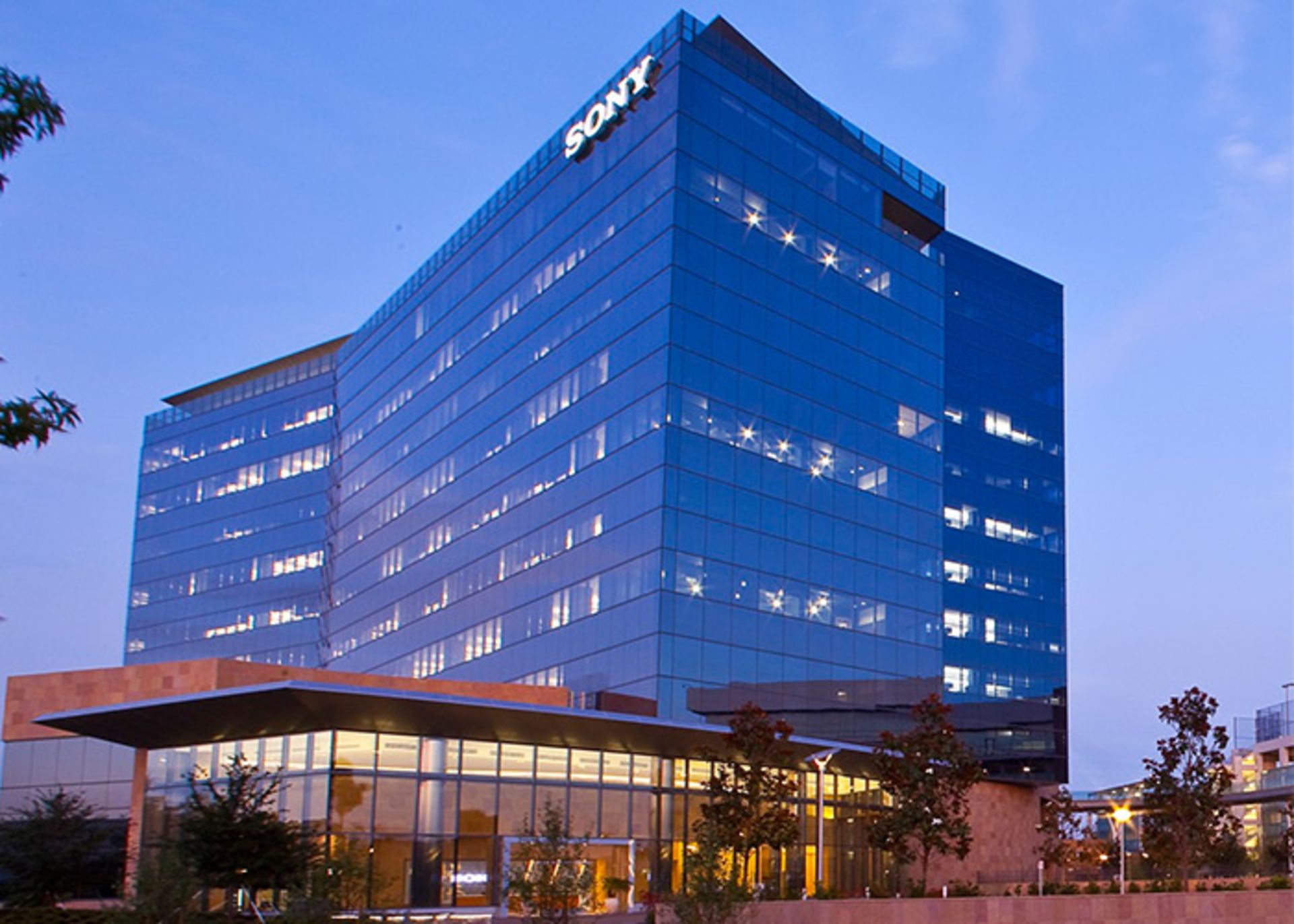
Sony Brand Story; From the production of rice cookers to becoming one of the most famous companies in the world
Noun: Someone who assists () a goal.
Sony brand story; From the production of rice cookers to becoming one of the most famous companies in the world
Sony is a Japanese multinational company headquartered in Minato, Tokyo. This company provides electrical services, gaming, entertainment, and financial services.
Sony is known as one of the pioneers in the production of electrical products and in recent years it has improved its position among the top companies in the world. Sony consists of many subsidiaries, the most famous of which are Sony Pictures, Sony Music, Sony Mobile, Sony Entertainment, and Financial Holding.
The story of the formation of the Sony brand
Masaru Ibuka returned to Tokyo from World War II in September 1945 to start a new job in the Japanese capital. He set up his workshop in an old, war-torn building with only eight employees. Their initial office walls were full of cracks and had no windows, but over time as their business progressed, the office building also improved.
In October of that year, Ibuka and his group launched a new company called Tokyo Tsushin Kogi, or Tokyo Institute of Communications Research. At that time, everyone was eager to work in the new company and wanted to use their engineering knowledge to rebuild Japan. However, no one knew where to start. Most of the employees were paid from Ibuka’s small savings and they had to work hard to survive.
The story of the formation of Sony goes back to 1945; When Masaru Ibuka returned from World War II
At that time and during the Second World War, people were thirsty to hear the news of the day. As a result, they came up with an interesting idea that changed the fate of the company forever. Most of the radios at that time were either destroyed by the war or could not receive radio waves due to police interference.
The Ibuka company repaired broken radios and also made it possible to receive waves using a series of converters. It didn’t take long for this model of radio to gain many fans among people.
Their business was in the center of attention and for this reason one of the Japanese newspapers published an article about them. This article not only got them more customers but also brought Ibuka’s old friend, Akio Morita, closer to him.
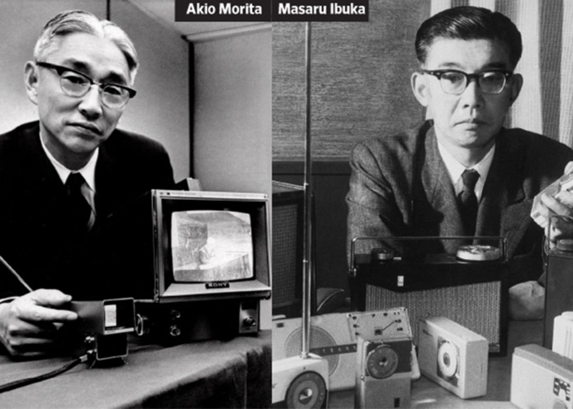
Ibuka and Morita, the founders of Sony Corporation, first met on a research committee studying new types of war weapons.
After some time passed, despite the big age difference, a deep friendship between Ibuka and Morita was formed. After the end of the war, Morita returned to his hometown and the communication between them was cut off. Until one day he read his friend’s name in a newspaper article and called Ibuka. Ibuka also asked him to get to Tokyo as soon as possible to start working with him again.
Sony’s brand name was originally supposed to be TTK or Totsuko
They were looking for a new name to advertise their company globally. Their intention was to choose the abbreviation of the company’s name, TTK, for advertising, but this name was already used. The word Totsuko was also another suggested name. But during his trip to America, Morita realized that it is difficult for Americans to pronounce this name.
They finally chose the name Sony from the combination of 2 words Sonus meaning sound and Sonny meaning young boy. Their purpose in choosing this name was to pronounce it in the same way in all languages of the world.
The company’s first product was a rice cooker, which, contrary to expectations, failed to meet expectations and failed. They did not get discouraged after their first failure and devoted more money to research. They focused on developing products that would benefit the Japanese people.
Sony; The first brand
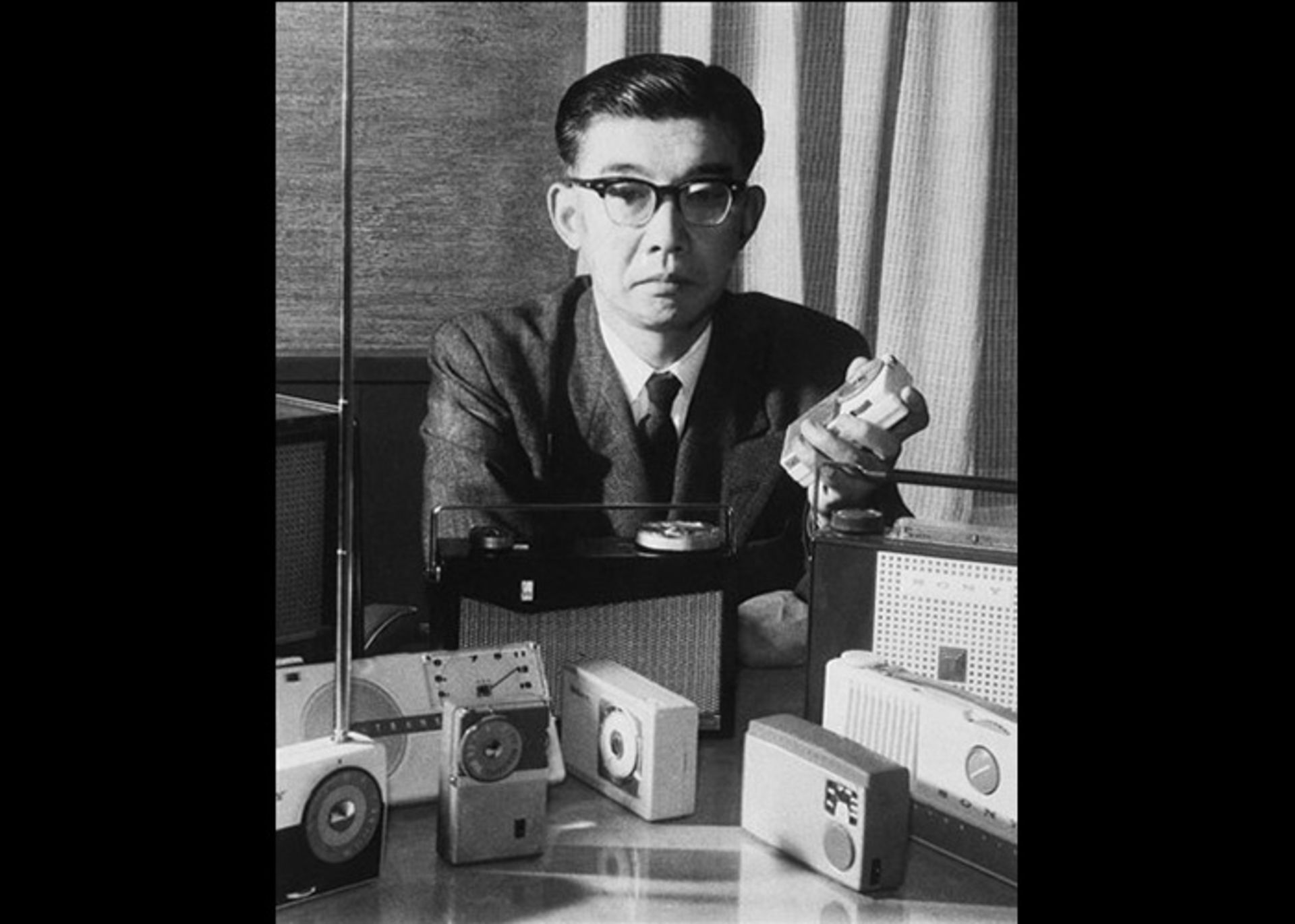
During 77 years of operation, Sony has been able to launch the first product in many markets of the world. From Japan’s first tape recorder to Japan’s first transistor radio and other products.
Tape recorder
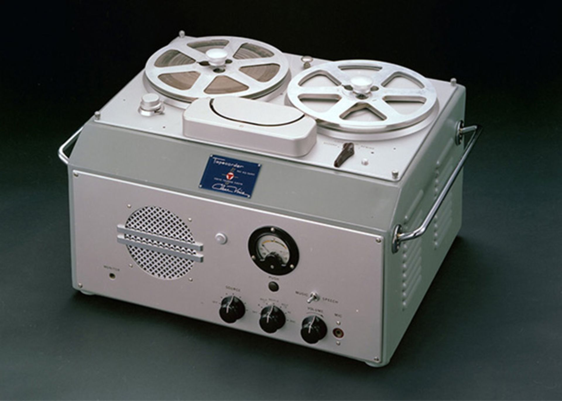
In 1950, the first Japanese tape recorder was made from its American model. This device was also not well received until Sony released a translated version of 999 Ways to Use the tape recorder.
After people became familiar with the product’s uses, the purchase request increased and the Sony tape recorder sold well. The demand for this product increased so much that the company had to expand its facilities to produce orders.
Transistor radio
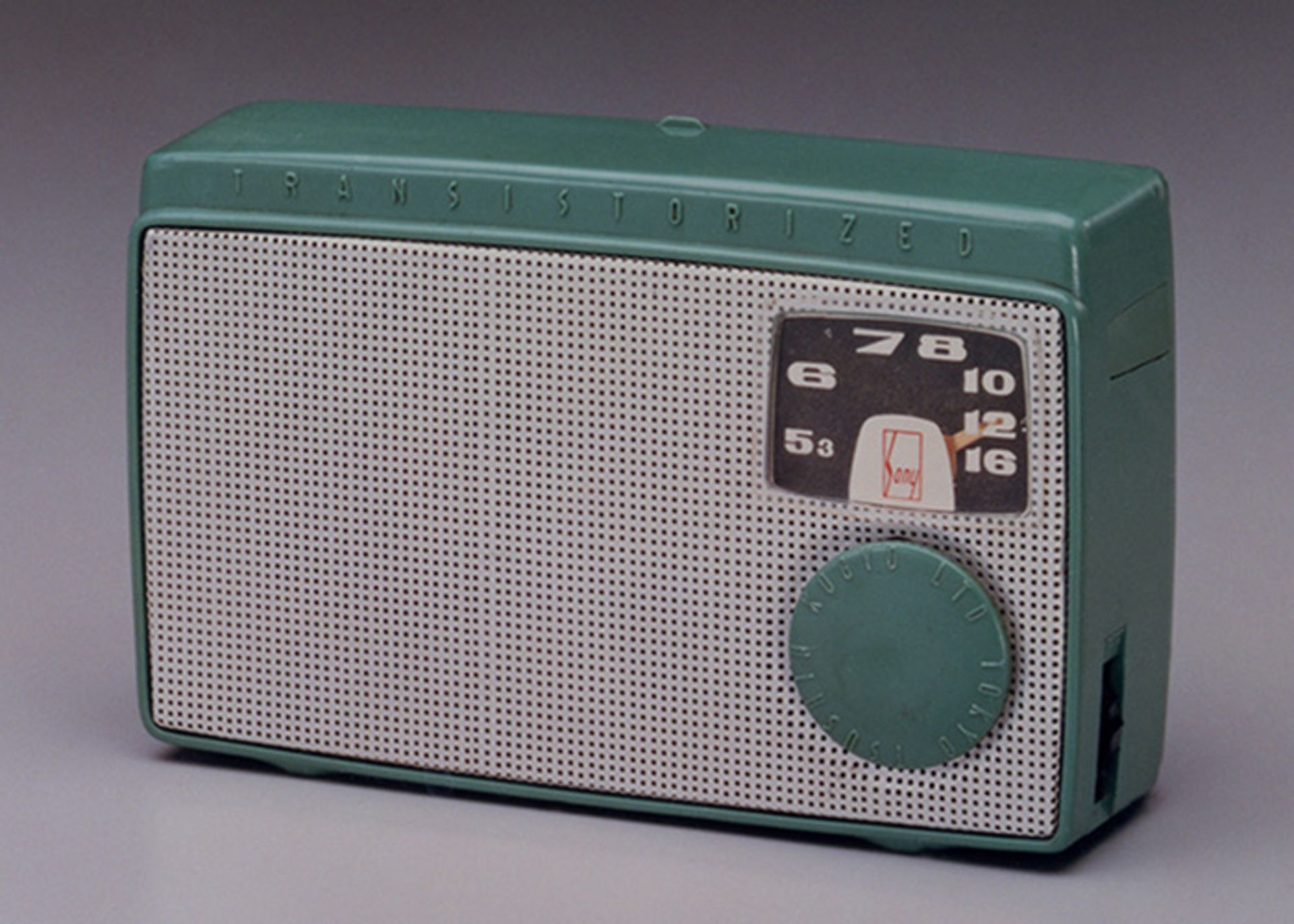
Japan’s first transistor radio was introduced in 1955 by Sony.
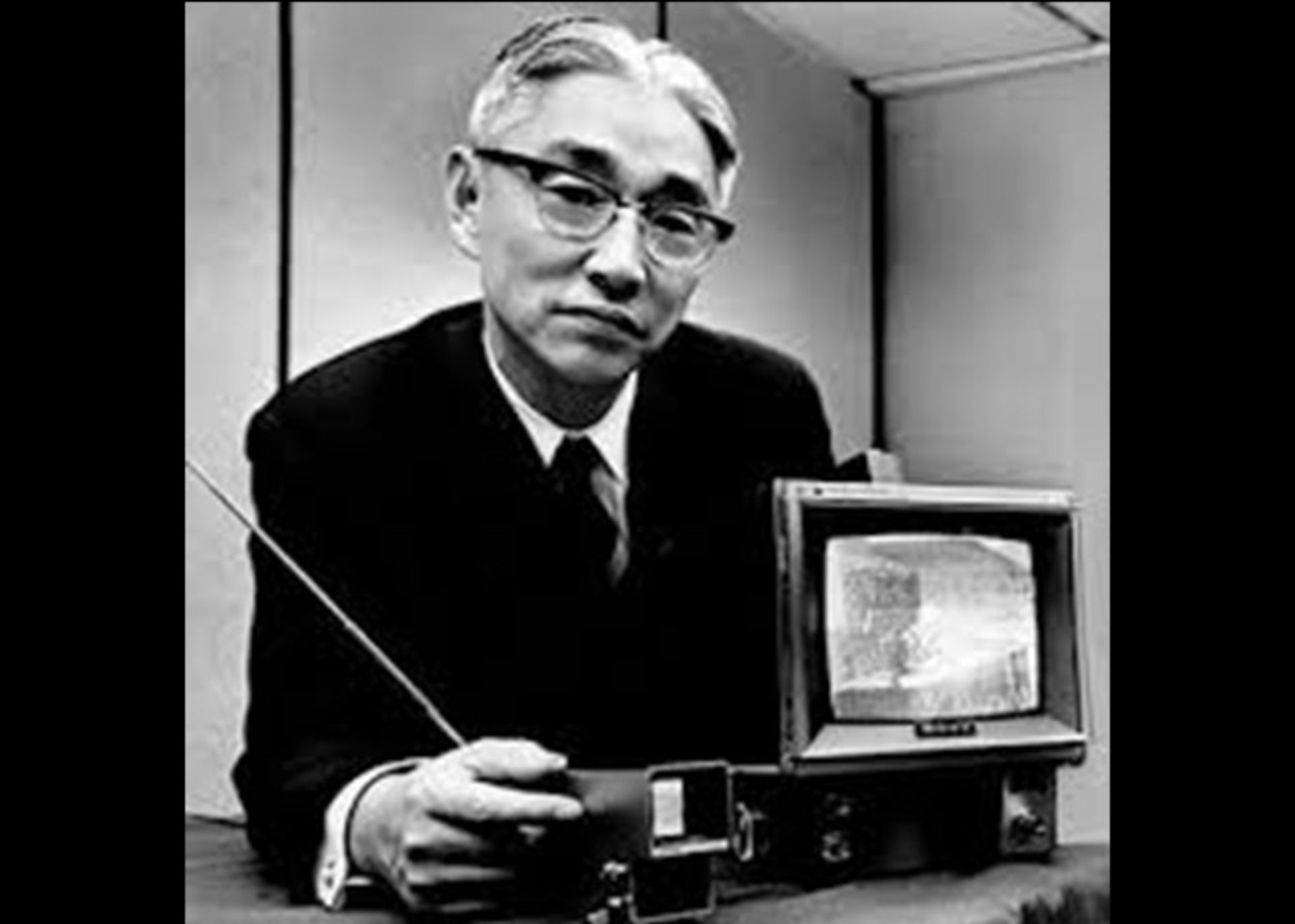
Portable TV
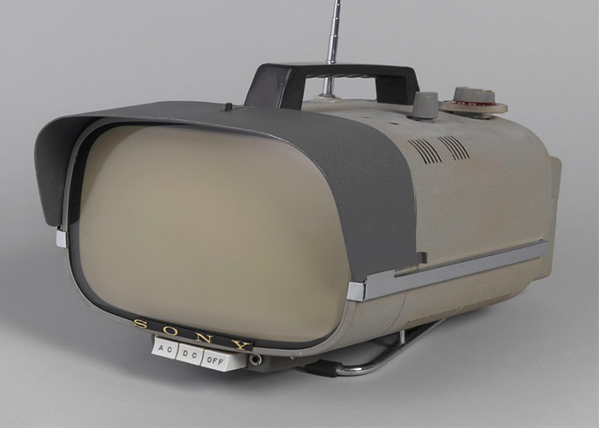
In 1960, Sony released the world’s first portable transistor TV. Sony used radio technology to produce this device.
The televisions of that time were big and in every house, a specific room was reserved for them. But these products brought a new definition of personal televisions to the market.
Video tape player
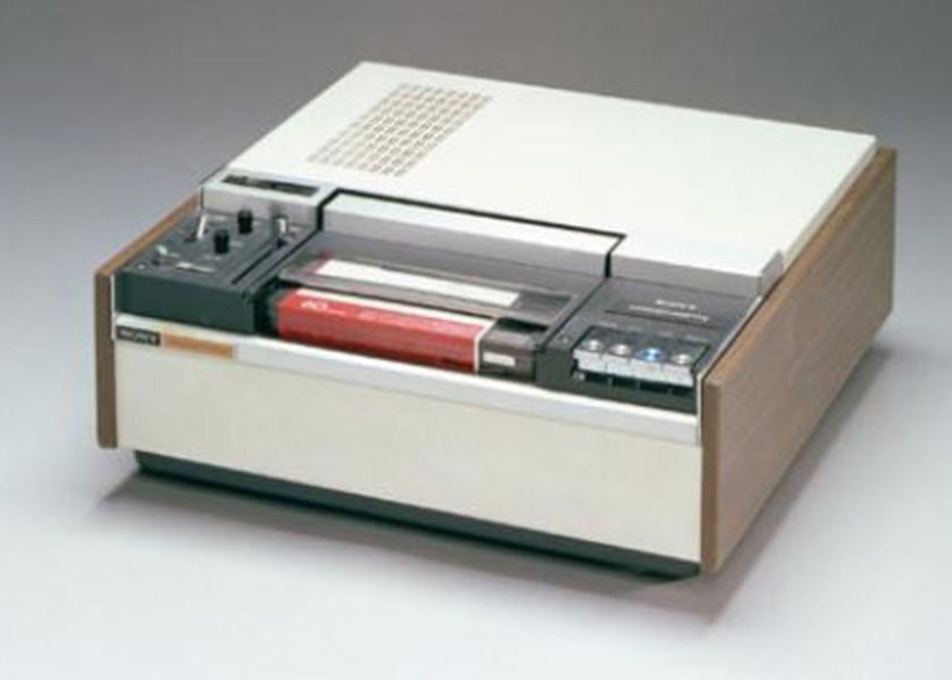
In 1971, Sony unveiled another product. This player was able to show videotapes in color inside the TV.
Masaru Ibuka retired in 1976 and was succeeded by Akio Morita as CEO.
The first generation Walkman
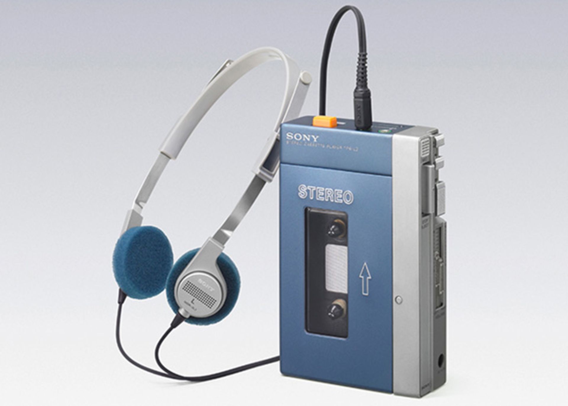
In 1979, Sony launched the first generation of Walkmans. These devices were portable and customers could listen to their favorite cassettes anywhere.
Many employees of the company believed that this device could not become popular among people without the ability to record sound. But contrary to their belief, this device introduced a new and successful lifestyle among people and achieved remarkable success.
The first CD player
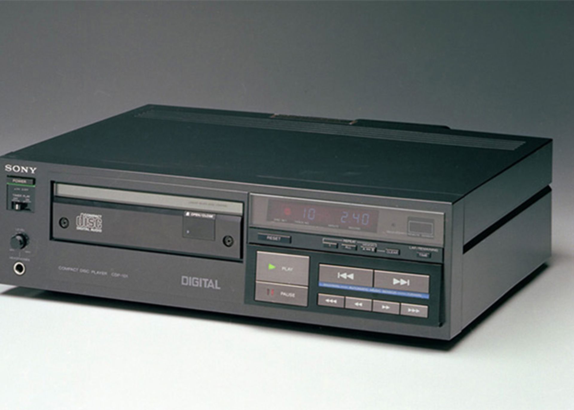
The world’s first CD player was launched in 1982 by Sony.
One of Sony’s senior managers, Norio Oga, was elected as the company’s CEO in 1989. Sony bought Columbia Pictures in the same year. This action was considered the biggest purchase of a Japanese company at that time.
PlayStation
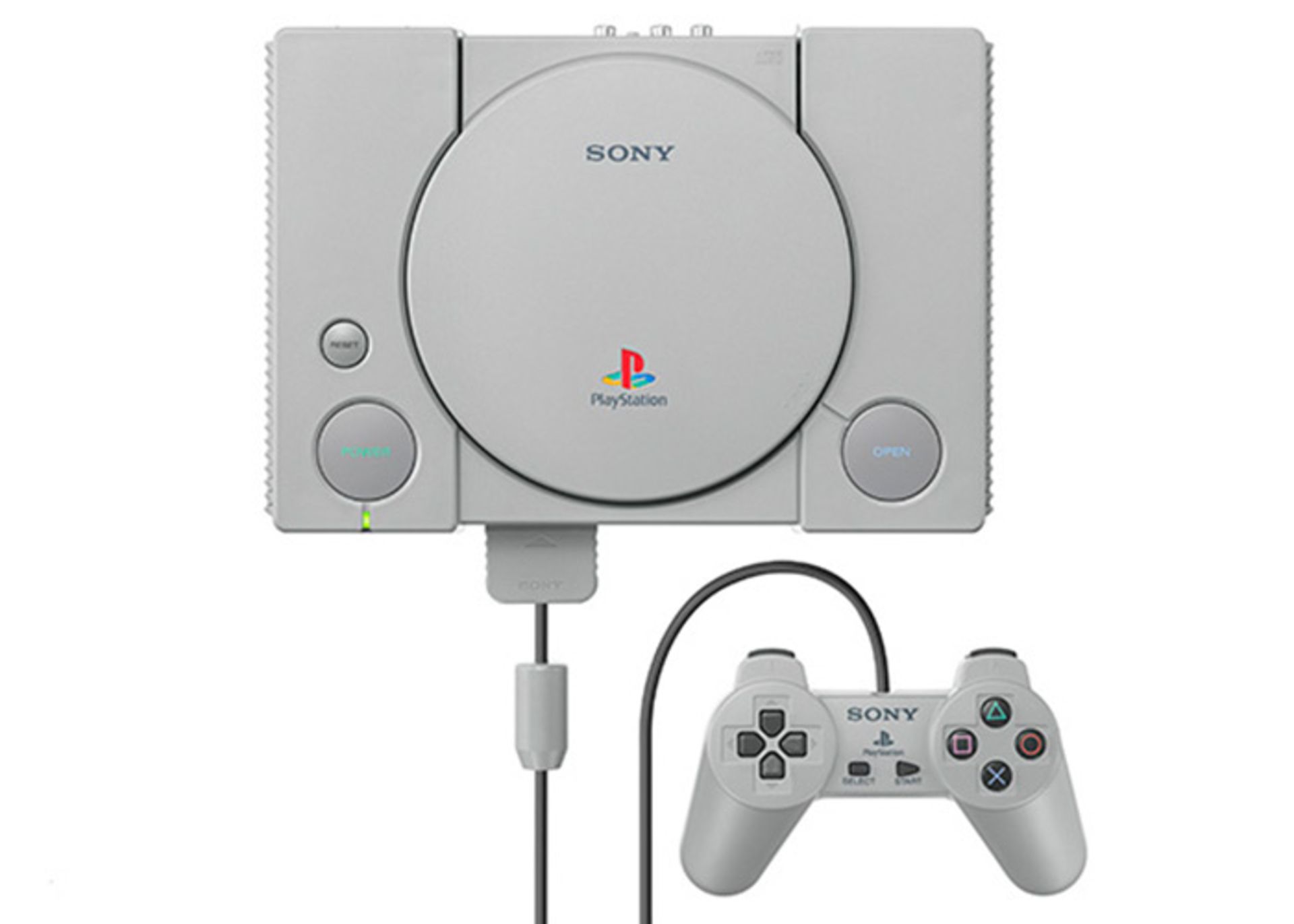
PlayStation is another important product of Sony. This product was sold in the Japanese market in 1994 and entered America and Europe in 1995.
PlayStation became so popular among people that its sales reached 10 million units by the end of 1996, and in 1998, about 50 million of this console had been sold. The production of new models of this product continues and today PlayStation 5 is considered the newest Sony console.
Digital camera
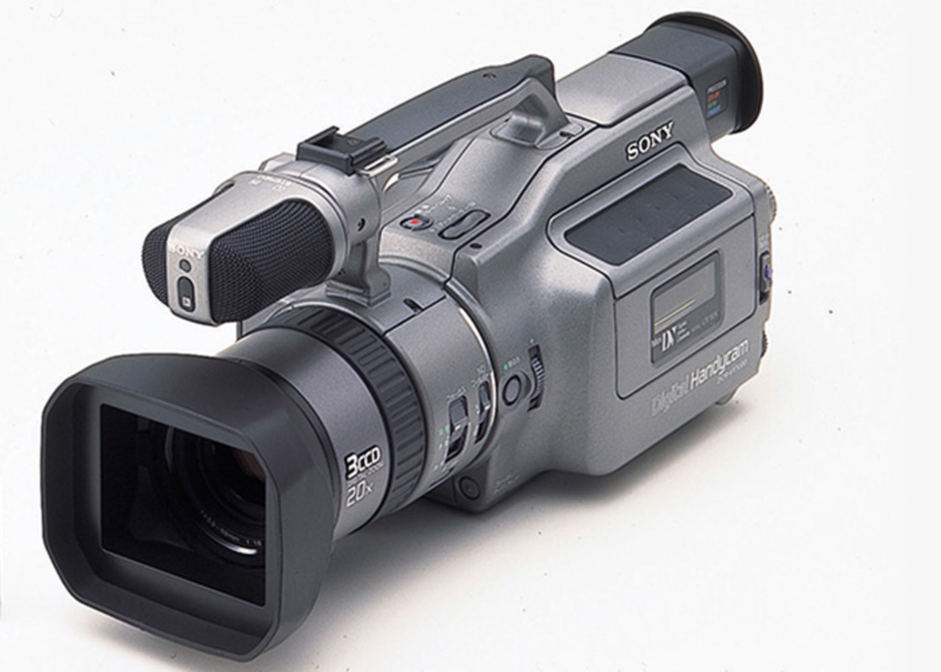
The first digital camera was launched by Sony in 1995. This device was very well built and recorded high-quality videos.
Sony Mobile
Sony Mobile Company started working in 2001 in cooperation with Ericsson. The company’s products were first marketed under the name of Sony Ericsson until Sony bought Ericsson’s shares in 2012. Since then, the phones of this company have entered the market under the name of Sony.
In 2012, Sony was able to win the title of the fourth mobile phone manufacturer. Xperia series mobile phones are the current flagships of this company. The Xperia brand doesn’t sell much at the moment, but Sony continues to produce products.
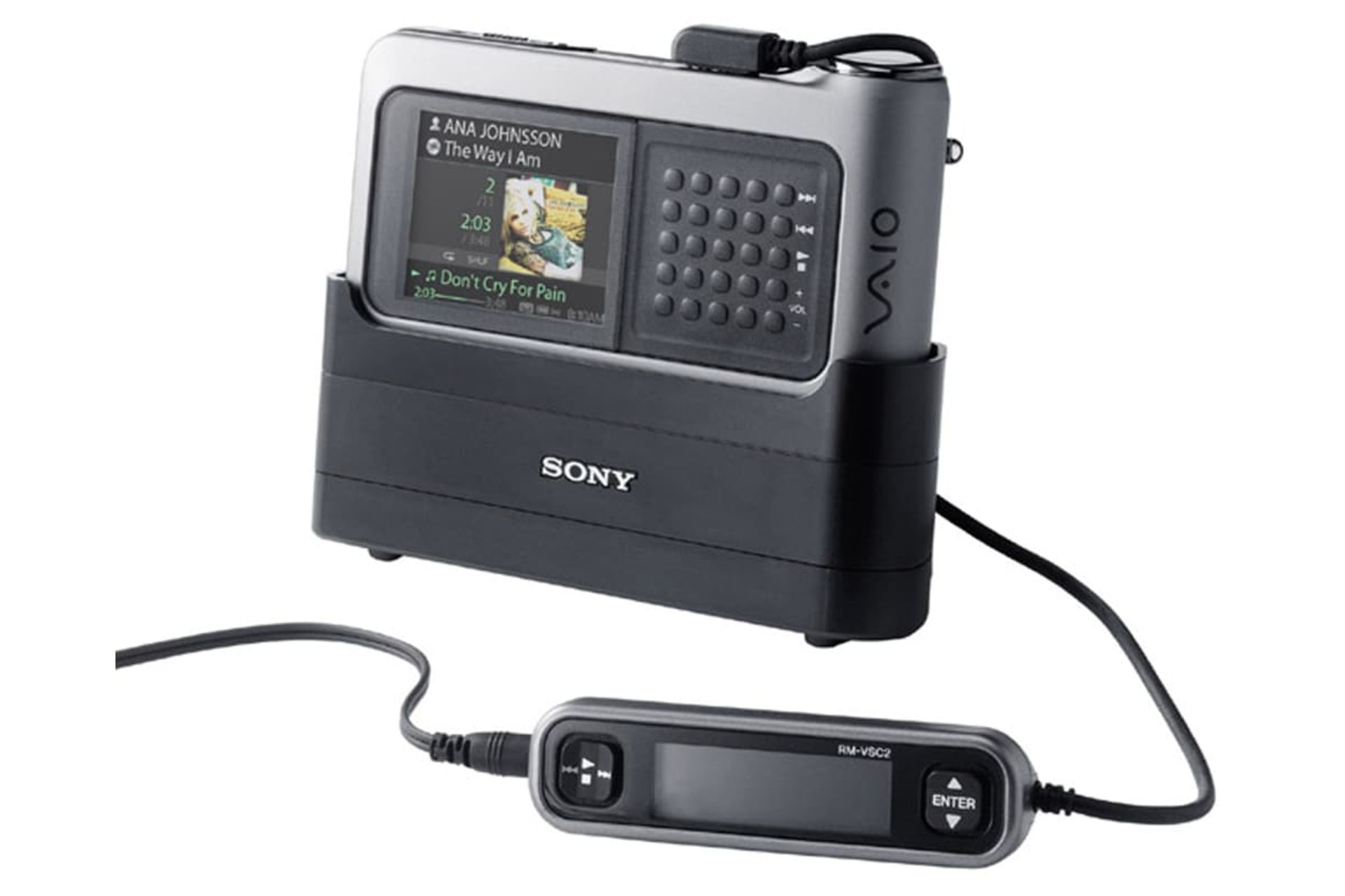
Vaio laptop
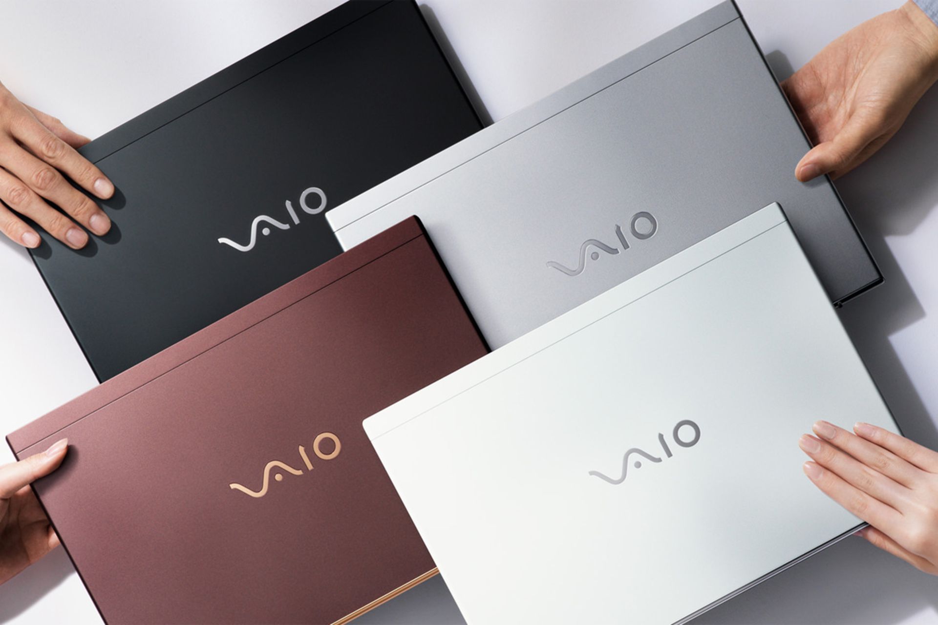
The first generation of Vaio laptops was launched in 1997. These laptops had a slim body and introduced a new concept of personal computers to the world.
Personal life of Masaru Ibuka
Masaru Ibuka was born on April 11, 1908 in Nikko, Japan. He graduated from the university in 1933 and worked in a film production company. Ibuka joined the Navy during World War II and was a member of the investigative committee; But after some time in 1945, he left the war to start his own radio repair workshop in Tokyo.
At that time, people followed the news of the world through the radio. As a result, starting a radio-related business was a good idea for a company. Ibuka and Akio founded Sony in 1946. Ibuka used transistors to make his company’s products. Therefore, Sony was introduced to the world as one of the first companies to use this technology for non-combat purposes.
Ibuka was a member of the Navy during World War II
In 1976, Ibuka was awarded an honorary doctorate from the University of Tokyo. He received two other honorary doctorate degrees in 1979 and 1994 from Tokyo and American universities.
Ibuka published a book titled “Kindergarten is Too Late” in 1971. In this book, he claimed that the most important time for human learning is from birth to three years old. As a result, he has suggested ways to teach skills to children at this time.
Ibuka was the leader of Sony until 1976 and then he retired; But even after that, he had a close relationship with company managers and guided them. He died in 1997 at the age of 89 due to heart failure.
Personal life of Akio Morita
Akio Morita was born on January 26, 1921 in Japan. He was the eldest of his four siblings. As a result, his father trained him to manage the family business.
Akio was very interested in mathematics and physics and graduated from university with a degree in physics. During World War II, he became a member of the Japanese Army’s Research Committee, and while serving, met his future business partner, Masaru Ibuka.
Morita was a huge fan of all Sony products and worked hard to promote them. For example, the size of their first production radios was slightly larger than the standard shirt pocket size. Because they wanted to market their products as pocket radios, Morita made shirts for their employees with larger pockets to show customers that these radios were pocket radios.
Sony established its first branch in America in 1960. Sony was the first Japanese company to enter the US stock market. In 1994, Morita suffered a stroke while playing tennis and resigned from the chairmanship of Sony. He finally died of pneumonia in 1999 at the age of 78.
Sony failures
Since its establishment in 1964, Sony has produced successful and innovative products. Many of these products were entering the market for the first time, and as a result, they introduced a new concept of technology to the world; But no success story is without failures.
Sony Aibo
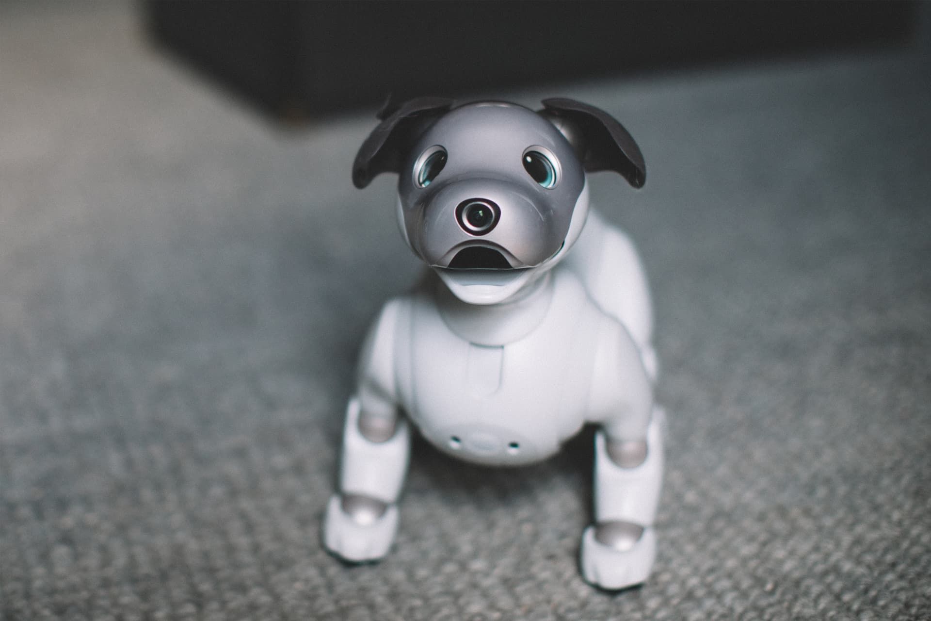
Sony robots were launched in 1999. These robots were in the form of cute dogs and had the power to learn. These robots could show emotions such as happiness, sadness, anger, surprise, fear and disinterest.
Sony robots were sold at a price of $2,500 and were very popular among their owners. But its high price prevented it from increasing its popularity and eventually, Sony stopped production.
Vaio music device
In 1979, Sony introduced a new concept of portability to the market by presenting its Walkman. The company had been Apple’s fierce competitor in digital music for two years, but its first product did not perform well.
The biggest mistake of the company was the dependence of files on the ATRACT format. Files with this format could only be used in Sony minidiscs. The ability to share files was the first word in digital music in 2000, and all files were released in MP3 format. As a result, this issue became a big challenge for Sony.
Sony e-Villa
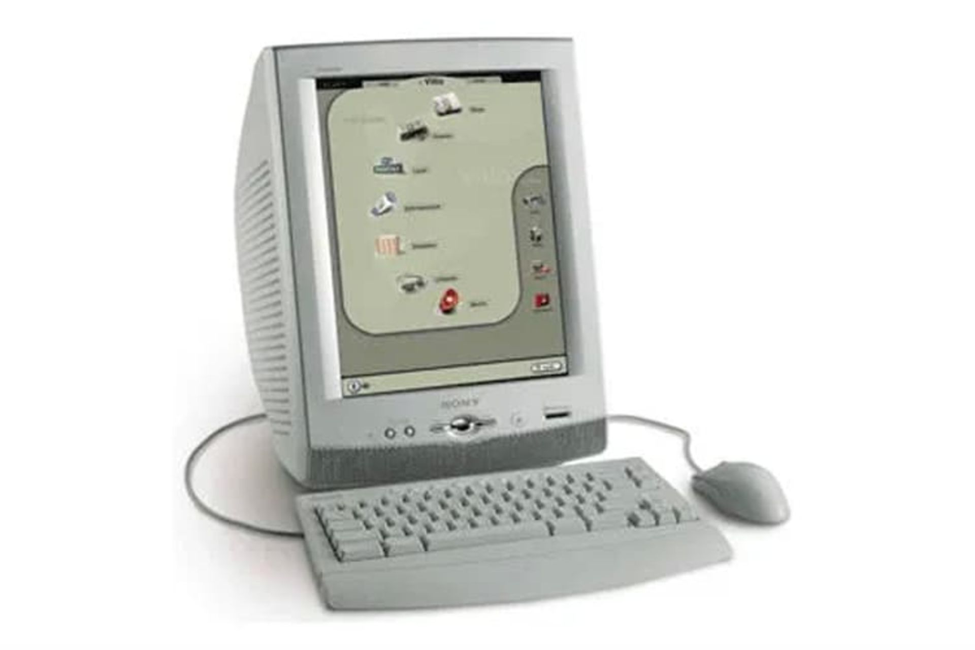
In 2001, many companies were offering Internet home appliances, including dedicated terminals for accessing the Internet and web browsers. Sony e-Villa was also a product that was launched with the same purpose.
The e-villa had a 15-inch monitor and a 56 kbps dial-up modem. e-Villa was designed to have access to email services and websites. At that time, there was a lot of competition between these devices and people preferred to use devices with Windows XP. As a result, Sony stopped the production of these products after three months.
Sony Airboard
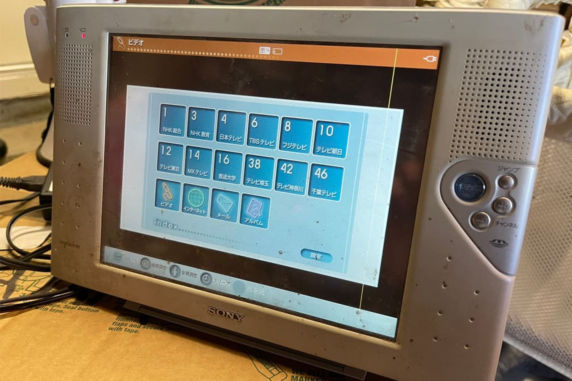
10 years before people became interested in watching videos on tablets, Sony launched a device called Airboard. The tablets of this family were 10 inches and had the possibility to connect to Wi-Fi and broadcast TV channels.
Using the picture-in-picture feature, users could search the Internet and watch TV. This device never caught on because people thought it was just a portable and expensive TV. Therefore, its production was stopped before entering the American market.
Sony PSX
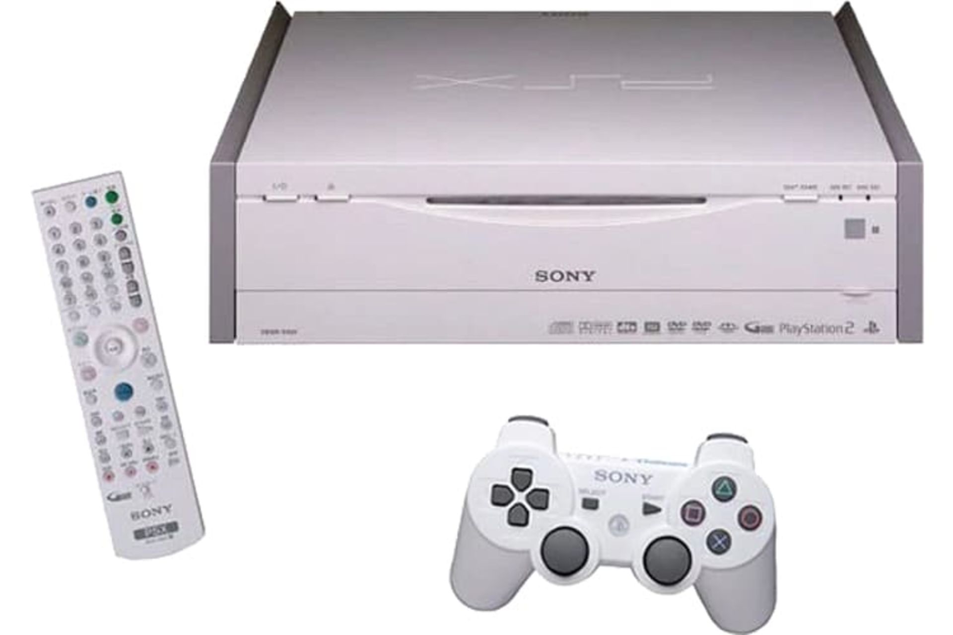
In 2003, Sony combined its two products, the PlayStation 2 and the video recorder, and marketed it as a single product. Using this product, customers could record the TV show on the storage memory or DVD at the same time as the game experience.
But the PSX, which was released only in Japan, was much larger and heavier than the PlayStation. Although this product did not have a high price, it could never attract many customers.
The current state of the Sony brand
Sony is one of the largest Japanese companies by revenue. The company reached the peak of profitability in the 1990s and 2000s due to the launch of its PlayStations, but faced financial problems in the late 2000s.
Read more: Samsung brand story; Full-view mirror of Korea’s commercial history
The global financial crisis, increased competition with PlayStation, and the earthquake in Japan in 2011 went hand in hand with Sony experiencing major failures for three years.
Due to the negative effects caused by natural disasters and exchange rates, the Times magazine called Sony a lack of flexibility and inability to measure the economy, but Sony was able to overcome all the crises in all these years by using innovation and became one of the top companies in the world. become in the television industry.
Sony’s current slogan is Be Moved, and the company aims to emotionally excite its customers with every product it offers.
Sony was able to pocket an operating profit of 1.21 trillion yen (about 8.9 billion dollars) in fiscal year 2022, which is a new record. Sony’s revenue in the final quarter of last year grew by 35 percent to about 3.06 trillion yen ($22.5 billion).
Adjective: The greatest; the best.
Pronoun: The greater part of a group, especially a group of people.
Noun: The greatest amount.
Noun: The greater part.
Noun: A record-setting amount.
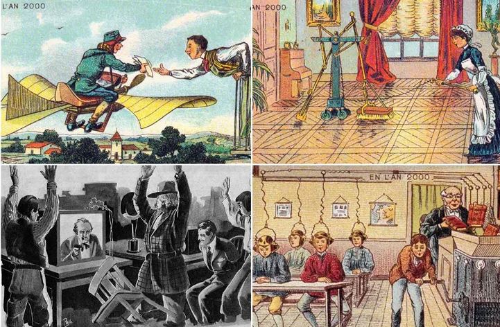
How did the people of the past imagine the future?
How can you explain to people in the 1900s that a robot can sweep floors and carpets without any intervention by drawing a map of your house without sounding crazy?
To people of the last century, our technology today seems like magic; But that doesn’t mean they didn’t fantasize about what the future would be like. Many inventors and artists have depicted their own predictions of future technology. Let’s look at these paintings and then comment on their scope.
 Bird postman – 1892
The potential of human flight was one of the concerns of futurists. It is true that aviation has revolutionized our world, but the type of flying equipment and “flying cars” that captured the imagination a century ago will remain for the future.
One of the important innovations that the minds of the ancients often did not imagine is the Internet and modern wireless communications. In today’s world, the flying postman pictured here would probably be out of a job thanks to plain old email.
 Electric floor washer (electric scrubber) – 1899 | The vacuum cleaner was invented just two years after this image was made.
The idea of a robot vacuum cleaner, now a reality in millions of homes, was apparently beyond imagination in the late 19th century.
 Machine learning-1901
According to this prediction, teaching was supposed to become a very easy job by the year 2000. The principal simply feeds the history books into the machine, while an assistant (or perhaps a student being punished?) turns the handle and somehow wires the contents of the books to the headsets the students are wearing, and from there into their minds. sends Do you understand the necessity of the presence of the school principal in this process?
 Phone with photo – 1918
The arrival of video-calling technology was predicted more than a century ago. The Electrical Experimenter magazine wrote in 1918: “Many inventors have attempted to invent a device or machine by which one person can see another while talking on the telephone.” According to the author of the magazine, such a device, which should naturally be called a “telephot”, will be invented sooner or later, because “everyone would like to have such a device.”
 Video call – 1942
Another article in the magazine Practical Electrics in 1942 predicted a similar device with moving pictures so interesting it is admirable.
 wheel of destruction
During World War I, specialized technology magazines were full of ideas that were hoped to bring an end to the long conflict. One of these inventions was the gyro-electric destroyer. “This 45-foot monster is steered by a large gyroscope wheel,” Electrical Experimenter magazine reported. “The destroyer travels at a speed of 40 to 60 miles per hour and because of its large diameter it easily rolls over trenches and other obstacles.”

The vision envisions a robot dog that readers can build for themselves; A wheeled device that operates with batteries and follows its owner’s metal cane through a magnet. It may have a cute face but don’t expect this dog to roll over, play, or react if something bad happens to you.
The idea of artificial pets doesn’t seem so strange nowadays. This is a concept that exists mostly in the field of cyberspace, exemplified by digital home assistants and artificial intelligence-based video game characters.
 Climate control – 1954
The dramatic image above shows how future humans will be able to control the weather. This article describes an airplane that is dispatched to disperse a cloud that threatens to form a tornado. “In the age of the hydrogen bomb and supersonic flight, it’s possible that science will find ways not only to destroy tornadoes and hurricanes but also to influence weather conditions in ways that will boggle the imagination,” the magazine reports.
Read more: The future of generative artificial intelligence from its own language
 Food planning by computer – 1967
In 1967, Philco-Ford, a maker of electrical goods, produced a short film called 1999AD, showing how its future products might transform ordinary homes. The family in the film owns a space-age car, a large wall-filling television, and a large home computer that helps the family (specifically the mother) plan their meals. In the film, we see the father of the family using the computer to check the invoice for the clothes he bought online.

Do animals have an understanding of the concept of death?

What is Kali Linux? Everything you need to know about this popular but mysterious distribution

Sony Brand Story; From the production of rice cookers to becoming one of the most famous companies in the world

How did the people of the past imagine the future?

Mammoth and dodo return to nature

Canopus; What do we know about the second brightest star in the sky?

How to use iMessage on Android?

Can humans endure the psychological torment of living on Mars?

Xiaomi Glorimi M2 Max watch review; Alternative economic option for iPhone owners

Artificial intelligence problems; Frauds based on artificial intelligence and methods to deal with them
-
 Technology1 year ago
Who has checked our Whatsapp profile viewed my Whatsapp August 2023
-
Technology1 year ago
Second WhatsApp , how to install and download dual WhatsApp August 2023
-
Technology1 year ago
How to use ChatGPT on Android and iOS
-
AI2 years ago
Uber replaces human drivers with robots
-
Technology1 year ago
The best Android tablets 2023, buying guide
-
Technology1 year ago
The best photography cameras 2023, buying guide and price
-
Humans2 years ago
Cell Rover analyzes the inside of cells without destroying them
-
Technology1 year ago
How to prevent automatic download of applications on Samsung phones